
Crystal structure is the unique, highly ordered arrangement of atoms, ions, or molecules in a crystalline solid. It is defined by a repeating unit called a unit cell, which extends in three-dimensional space to form a lattice. This structural arrangement determines a material’s physical, electrical, and thermal properties.
Core Principles of the Crystal Structure
Crystal structure forms when a mathematical lattice combines with a physical basis of atoms. It represents how particles pack together to minimize energy and maximize stability in a solid. Understanding this geometry is essential for solid state physics, as it explains why materials like diamond and graphite behave differently despite having identical atoms.
In the study of solids, the lattice is a purely theoretical collection of points that repeat periodically. When you place an atom or a group of atoms—known as the basis—on every lattice point, you generate the actual crystal structure. This distinction is vital for competitive exams because questions often distinguish between the symmetry of the lattice and the symmetry of the actual atomic arrangement.
The periodic nature of a crystal structure allows scientists to describe a massive bulk material by looking at just a tiny segment. This repeating segment is the unit cell. By analyzing the symmetry and dimensions of this cell, we can predict how the material will react to stress, heat, or electricity. This predictable behavior is what makes crystalline solids distinct from amorphous solids like glass, which lack a long-range ordered crystal structure.
Analysis of Fundamental Unit Cell Types
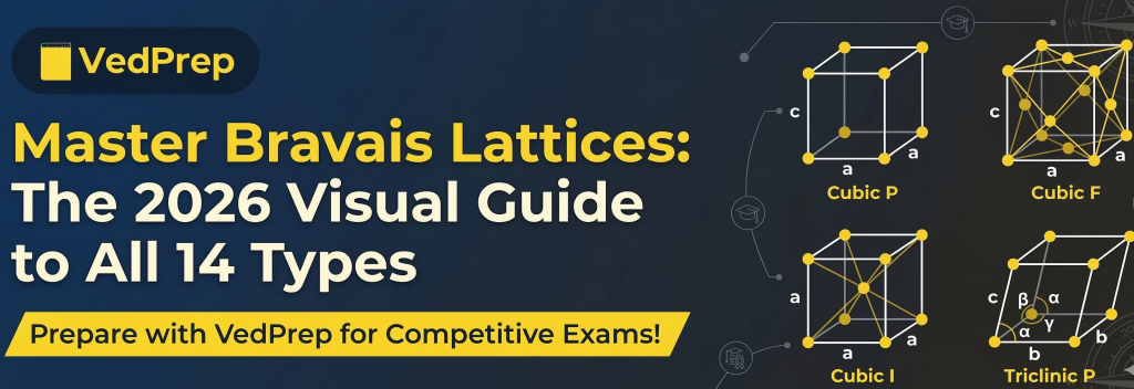
Unit cell types are the smallest repeating building blocks of a crystal structure that represent the overall symmetry of the entire solid. These include Primitive, Body-Centered, Face-Centered, and End-Centered cells. Identifying the correct unit cell is the first step in calculating material density and understanding atomic arrangements in three dimensions.
The Primitive (P) cell is the simplest of the unit cell types, containing lattice points only at the corners. In contrast, a Body-Centered (I) cell includes an additional point at the center of the volume. Face-Centered (F) cells feature points at the center of each of the six faces, while End-Centered (C) cells have points only on two opposite faces.
For students of solid state physics, mastering these unit cell types is necessary for calculating the “effective number of atoms” (Z) per cell. For example, a simple cubic cell has Z=1, while a Face-Centered Cubic cell has Z=4. These values are non-negotiable for solving numerical problems regarding density and atomic radius. Most competitive exam errors occur when students confuse the total number of atoms visible in a diagram with the actual shared contribution of atoms within the unit cell boundaries.
The Seven Crystal Systems and Bravais Lattice Guide
The seven crystal systems categorize all possible crystal structures based on their axial lengths and interaxial angles. These systems include Cubic, Tetragonal, Orthorhombic, Hexagonal, Rhombohedral, Monoclinic, and Triclinic. Combined with centering types, they form the 14 Bravais lattices, which provide a complete Bravais lattice guide for classifying every periodic solid.
Each of the seven crystal systems is defined by six parameters: three edge lengths (a,b,c) and three angles (α,β,γ). The Cubic system is the most symmetrical, where a=b=c and all angles are 90∘. Conversely, the Triclinic system is the least symmetrical, with no equal sides or angles. These classifications are the primary framework used in X-ray diffraction analysis to identify unknown minerals and alloys.
A comprehensive Bravais lattice guide helps researchers understand that not every centering type is possible for every system. For instance, the Tetragonal system only supports Primitive and Body-Centered lattices. There is no such thing as a Face-Centered Tetragonal lattice because that geometry can always be simplified into a smaller Body-Centered Tetragonal cell. Understanding these geometric constraints is a common “trap” in advanced physics papers and GATE examinations.
Calculating Atomic Packing Factor and Coordination Number
The atomic packing factor (APF) measures the efficiency of space utilization within a crystal structure, calculated as the ratio of atomic volume to unit cell volume. The coordination number table lists how many nearest neighbors surround a central atom. These values are critical for predicting the density and structural integrity of metals.
The atomic packing factor tells us how “tightly” atoms are squeezed together. In a Simple Cubic structure, the APF is only 0.52, meaning nearly half the space is empty. However, in a Hexagonal Close Packed or Face-Centered Cubic arrangement, the APF reaches 0.74, which is the maximum possible packing efficiency for equal-sized spheres. High packing efficiency generally correlates with higher material density and stability.
A coordination number table is an essential tool for identifying the bond strength of a crystal structure. In a BCC lattice, the coordination number is 8, while in FCC and HCP systems, it is 12. A higher coordination number often indicates a more closely packed environment. When solving exam problems, always remember that the coordination number depends strictly on the geometry of the lattice and the specific unit cell types involved in the structure.
X-ray Diffraction Analysis in Solid State Physics
X-ray diffraction analysis is the primary experimental technique used to determine an unknown crystal structure. By measuring the angles and intensities of diffracted beams, researchers can calculate interplanar spacings using Bragg’s Law. This method is the backbone of solid state physics, allowing scientists to map the precise coordinates of atoms in a lattice.
When X-rays hit a crystal structure, they are scattered by the electron clouds of the atoms. If the waves remain in phase, they interfere constructively, creating a bright spot on a detector. This phenomenon is described by the equation nλ=2dsinθ. By analyzing these patterns, crystallographers can determine the exact dimensions of the seven crystal systems present in a sample.
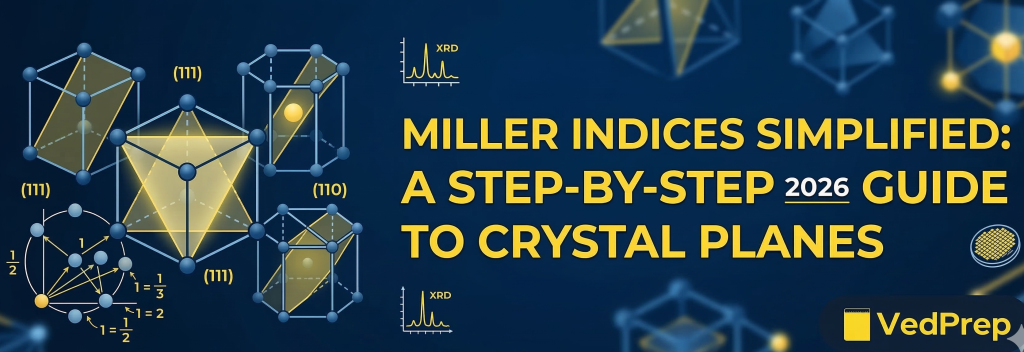
In the realm of solid state physics, this technique does more than just identify materials; it reveals how a crystal structure changes under stress or temperature shifts. Modern laboratories now use automated software to match diffraction data against a global database of Bravais lattices. For students, understanding the relationship between the Miller indices (hkl) and the interplanar spacing (d) is the key to mastering diffraction problems in competitive tests.
Characteristics of Hexagonal Close Packed Structures
The Hexagonal Close Packed (HCP) structure is a high-density arrangement common in metals like Magnesium and Zinc. It features a repeating layer sequence of ABAB, distinct from the ABCABC sequence found in Face-Centered Cubic structures. Understanding the Hexagonal Close Packed geometry is vital for explaining why certain metals are less ductile than others.
[Image comparing HCP and FCC atomic stacking sequences]
In a Hexagonal Close Packed crystal structure, the unit cell is not a simple hexagon but a rhombic prism that represents one-third of the full hexagonal shape. The coordination number for this system is 12, and it shares the same maximum atomic packing factor of 0.74 with the FCC system. However, the symmetry of the HCP lattice provides fewer “slip planes,” which is why HCP metals tend to be more brittle than FCC metals like Gold or Copper.
The calculation of the c/a ratio is a unique requirement for the Hexagonal Close Packed system. In an ideal scenario where atoms are perfect spheres, this ratio is approximately 1.633. Deviations from this value indicate that the atoms are slightly distorted, affecting the physical properties of the metal. This specific detail is a frequent topic in advanced solid state physics modules and materials science interviews.
Advanced Crystal Symmetry Groups and Mathematical Order
Crystal symmetry groups are mathematical descriptions that classify crystals based on their internal symmetry operations, such as rotation, reflection, and inversion. There are 32 point groups and 230 space groups that define every possible crystal structure. These groups allow scientists to predict a material’s optical and piezoelectric properties without conducting physical experiments.
Symmetry is the language of crystallography. While the seven crystal systems provide a basic shape, crystal symmetry groups describe the specific “instructions” for placing atoms within that shape. For example, some structures have a center of inversion, while others do not. This lack of a center of inversion is exactly what allows certain crystals to generate electricity when squeezed—a phenomenon known as the piezoelectric effect.
For exam preparation, you don’t need to memorize all 230 space groups, but you must understand the basic symmetry operations: rotation (Cn), reflection (σ), and inversion (i). These operations help in identifying which of the seven crystal systems a material belongs to. If a crystal structure possesses a four-fold rotation axis, it likely belongs to the Cubic or Tetragonal systems, narrowng down the possibilities for identification.
The Future of Material Science: Structure Prediction AI
Structure prediction AI uses machine learning and neural networks to simulate and discover new stable materials without extensive lab testing. By analyzing known crystal symmetry groups, these algorithms predict how atoms will organize under extreme pressures or temperatures. This technology is revolutionizing material science by accelerating the development of next-generation superconductors.
In 2026, researchers no longer rely solely on trial-and-error in the lab. Instead, structure prediction AI can scan millions of hypothetical atomic combinations to find a crystal structure with specific desired properties, such as high-temperature superconductivity. These AI models are trained on vast datasets of X-ray diffraction analysis results and known Bravais lattices to ensure their predictions are physically viable.
This computational approach is particularly useful for finding “metastable” phases arrangements that don’t occur naturally but can be created under specific laboratory conditions. By predicting the atomic packing factor and coordination number of these new materials, AI helps engineers design lighter alloys for aerospace and more efficient cathodes for electric vehicle batteries. For students, this highlights the growing intersection between computer science and solid state physics.
Why Geometric Perfection Often Fails in Reality
While textbooks describe an ideal crystal structure, real-world materials always contain defects like vacancies, dislocations, or impurities. Relying solely on perfect lattice models can lead to incorrect predictions of material strength or conductivity. Engineers must account for these “imperfect” realities to design reliable components for aerospace and electronics industries.
In an ideal model, every lattice point is occupied by the correct atom. In reality, a “vacancy” might occur where an atom is missing, or an “interstitial” defect might appear where an extra atom is squeezed into a gap. These flaws are not always bad; for example, the entire semiconductor industry relies on “doping,” which is the intentional introduction of impurities into a crystal structure to change its electrical behavior.
When students solve problems involving the atomic packing factor, they often assume a perfect 100% occupancy. However, a critical thinking approach requires acknowledging that the theoretical density is almost always higher than the measured density due to these microscopic voids. Understanding the limitations of the “perfect crystal” model is what separates an elite student from one who simply memorizes formulas.
Case Study: Enhancing Semiconductor Efficiency via Lattice Matching
Modern microchips rely on growing thin layers of one crystal structure atop another, a process known as epitaxy. If the unit cell dimensions do not match perfectly, strain occurs, leading to electronic failure. By choosing materials with compatible Bravais lattices, engineers can create high-speed transistors used in 2026 quantum computing processors.
Consider the development of Gallium Nitride (GaN) semiconductors. GaN has a Hexagonal Close Packed structure. To grow high-quality GaN crystals, researchers often use a Sapphire substrate, which also has hexagonal symmetry. If the distance between atoms in the GaN lattice (parameter a) is too different from the Sapphire lattice, the resulting crystal will “crack” at the atomic level, rendering the chip useless.
By utilizing structure prediction AI and precise X-ray diffraction analysis, engineers can calculate the exact “lattice mismatch.” They sometimes introduce a “buffer layer” of a third material to transition between the two different unit cell types. This meticulous management of the crystal structure is the secret behind the efficiency of modern LEDs, fast-charging bricks, and 5G communication towers.