
Scanning and transmission microscopes are advanced imaging tools used in materials science and nanotechnology to study the structure and properties of materials at the nanoscale. Understanding these microscopes is critical for CSIR NET aspirants, particularly when studying Electron Imaging Systems For CSIR NET.
Overview: Scanning and transmission microscopes For CSIR NET
If you are gearing up for the CSIR NET Physical Sciences exam, you already know that Unit 3 (Materials Science and Nanostructures) isn’t just about memorizing formulas. It is about visualizing things you can’t actually see with the naked eye. That is where electron imaging systems come into play. Specifically, mastering Scanning and transmission microscopes is an absolute must if you want to lock in those crucial marks in Part C.
Think of these Scanning and transmission microscopes as the ultimate high-powered cameras of the nanoworld. When you are looking at materials fabricated at the nanoscale, standard light microscopes are useless because of the diffraction limit of light. If you want to understand how a material behaves, you have to change how you look at it.
For a solid foundation, standard textbooks like Materials Science by Ranganathan are a great place to start. It covers the core physics of electron-matter interactions without getting bogged down in overly dense jargon. This topic also overlaps heavily with Section B of the IIT JAM Physics syllabus and crops up frequently in GATE. So, mastering it now gives you a massive advantage across multiple competitive exams.
Understanding Scanning and transmission microscopes For CSIR NET
Let’s break down how these two systems actually work. Imagine you are trying to study a massive, mysterious castle in the dark.
Scanning Electron Microscopy (SEM): This is like taking a high-powered flashlight and scanning it across the outside walls of the castle. The light bounces off the bricks, rocks, and crevices, giving you a beautiful, 3D-like picture of the surface texture, ridges, and valleys. In the lab, SEM does exactly this by sweeping a focused beam of electrons across a sample’s surface to map its topography.
Transmission Electron Microscopy (TEM): Now, imagine you want to know what is inside the castle walls—like the hidden rooms or structural beams. You’d need a beam so incredibly powerful that it shoots right through the walls. The parts where the wall is thick or dense will block the beam, while the thinner parts let it pass through, casting a shadow puppet image on the other wall. TEM shoots electrons right through an ultra-thin sample, giving you a 2D look at its internal crystal structure and defects.
The Golden Rule for Exams: SEM = Surface & 3D Topography. TEM = Internal Structure & 2D Projection.
Worked Example: Scanning and Transmission Microscopes in CSIR NET
When you see a question on this topic in the CSIR NET exam, it usually tests your grasp of electron optics or how electrons interact with matter. Let’s look at a typical problem style you might face.
Example Question
What is the primary difference between the operating mechanism of a scanning electron microscope (SEM) and a transmission electron microscope (TEM)?
How to approach it
To answer this, you need to think about what happens to the electron beam.
SEM relies on scattered electrons (like secondary or backscattered electrons) that knock off or bounce from the surface.
TEM relies on transmitted electrons that pass straight through the specimen.
Because of this, Scanning and transmission microscopes requires minimal sample preparation but gives you surface details. TEM requires the sample to be incredibly thin (often less than 100 nm) so the electrons don’t just get absorbed and stuck. At VedPrep, we always remind our students to focus on these operational constraints, as CSIR love to frame conceptual questions around sample thickness and beam voltage.
Common Misconceptions About Scanning and Transmission Microscopes For CSIR NET
A major trap candidates fall into is thinking that SEM is only good for looking at pretty 3D surface pictures. That is a bit of a myth. While SEM is famous for surface topography, it can also give you deep insights into chemical composition. For instance, by analyzing the X-rays knocked loose by the electron beam, you can figure out exactly what elements are sitting on that surface.
Another common slip-up is assuming TEM is only for looking at big, bulk pieces of material. In reality, it is completely the opposite. TEM cannot handle bulk materials at all. If your sample is too thick, the electron beam gets choked out, and you get nothing but a black screen. You have to slice your sample down to an atomic scale to get any useful data.
Application of Scanning and Transmission Microscopes in Materials Science
To make this click, let’s look at a fictional, real-world style scenario.
Imagine a team of materials scientists trying to develop a next-generation flexible smartphone screen. They need a coating that is scratch-resistant on the outside but perfectly conductive on the inside.
First, they would use SEM to check the outer surface. If the coating looks like a cracked desert floor under the microscope, they know it will peel off easily. The SEM helps them fix the surface texture and roughness.
Next, they need to know why the screen isn’t conducting electricity well. They slice a tiny, nanometer-thin cross-section of the screen and put it under a TEM. Here, they can see individual rows of atoms. They notice that the copper atoms aren’t lining up right; there are structural dislocations blocking the electrical current.
By using both Scanning and transmission microscopes, they fix both the outside and the inside of their material.
Exam Strategy for Scanning and transmission microscopes For CSIR NET
When you are diving into your revision, do not just read the text passively. You need to focus heavily on the mathematical side of things.
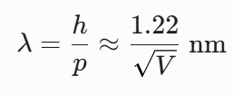
Master the Resolution Formula: Make sure you can comfortably work with Abbe’s resolution criterion and the de Broglie wavelength equation:
Understand Contrast Mechanisms: Learn the difference between mass-thickness contrast and diffraction contrast in TEM.
Practice Data Interpretation: CSIR NET questions often give you an electron diffraction pattern (like SAED dots or rings) and ask you to identify the crystal structure (FCC, BCC, etc.).
A great way to practice is to study actual micrographs. At VedPrep, we suggest active recall: look at a TEM diffraction pattern and practice indexing the planes yourself instead of just reading the answer key.
Real-World Applications of Scanning and Transmission Microscopes For CSIR NET
Beyond pure materials physics, these instruments drive major industries. In the semiconductor world, microchips are now so tiny that transistors are only a few nanometers wide. Companies use SEM daily to inspect these chips for tiny manufacturing errors.
Meanwhile, in structural biology and virology, TEM is the gold standard. When scientists are trying to map the spikes on a new virus to build a vaccine, light microscopes are completely blind to things that small. They rely on cryogenic TEM to freeze the virus mid-motion and take high-resolution snapshots of its internal machinery.
Key Features and Limitations of Scanning and Transmission Microscopes For CSIR NET
Here is a quick, no-nonsense comparison to help you keep the facts straight for the exam:
| Feature | Scanning Electron Microscope (SEM) | Transmission Electron Microscope (TEM) |
| Resolution | Typically 1–10 nm | Down to 0.1 nm (Atomic resolution) |
| Image Type | 3D surface view | 2D internal projection |
| Sample Prep | Simple; just needs to be conductive (often gold-coated) | Highly tedious; must be ultra-thin (<100 nm) |
| Information | Topography, morphology, composition | Crystal structure, defects, lattice imaging |
| Deflection | Magnetic lenses scan the beam across | Magnetic lenses focus the transmitted beam |
Advancements in Scanning and Transmission Microscopes Technology For CSIR NET
The world of electron imaging isn’t standing still. One of the coolest fields right now is correlative light and electron microscopy (CLEM). This technique lets researchers take a living cell, track its movement under a standard fluorescent light microscope, and then instantly freeze it to look at its atomic gears using a TEM.
We are also seeing massive upgrades in aberration-corrected TEMs. In the past, magnetic lenses had built-in flaws that blurred the images at ultra-high magnifications. Modern correction systems act like a pair of prescription glasses for the microscope, pushing the resolution limits well below a single angstrom.
Conclusion
Mastering the mechanics of Scanning and transmission microscopes is all about shifting your perspective. Instead of treating this topic like a checklist of facts to memorize before exam day, try to think about the physical principles at play—how electrons move, bend, scatter, and pass through matter. As per Scanning and transmission microscopes, understanding the technical mechanisms of microscopes is necessary to score high.
As the exam patterns shift toward more analytical, application-based questions, being able to interpret a microscope’s output is what will set you apart. Keep practicing those numerical problems on resolution and accelerating voltage. If you ever feel stuck on how these imaging systems function or need a structured way to tackle the physical sciences syllabus, the team at VedPrep is always here to help you break it down step by step.
To know more in detail from our faculty, watch our YouTube video:
Frequently Asked Questions
How does a transmission electron microscope (TEM) work?
A TEM works by transmitting a beam of electrons through a thin sample, producing an image of the sample's internal structure. The TEM provides high-resolution images of the sample's morphology and ultrastructure.
What is the primary function of a scanning electron microscope (SEM)?
The primary function of an SEM is to produce high-resolution images of a sample's surface topography. It works by scanning a focused beam of electrons across the sample, detecting signals emitted from the sample's surface.
What are the advantages of using electron microscopes over optical microscopes?
Electron microscopes have higher resolution and magnification than optical microscopes, allowing for detailed imaging of nanoscale structures. They are particularly useful for studying the ultrastructure of cells and biological molecules.
What are the applications of scanning and transmission microscopes in biology?
Scanning and transmission microscopes have various applications in biology, including studying cell morphology, ultrastructure, and molecular structure. They are used in fields such as cell biology, microbiology, and structural biology.
How do scanning and transmission microscopes contribute to our understanding of biological systems?
Scanning and transmission microscopes provide valuable insights into the structure and function of biological systems, from the molecular to the cellular level. They help researchers understand biological processes, interactions, and mechanisms.
How are scanning and transmission microscopes relevant to the CSIR NET exam?
Scanning and transmission microscopes are relevant to the CSIR NET exam as they are important tools in biological research. Questions related to these microscopes may appear in the exam, particularly in the cell biology and molecular biology sections.
What types of questions can be expected on scanning and transmission microscopes in the CSIR NET exam?
Questions on scanning and transmission microscopes in the CSIR NET exam may include their principles, applications, advantages, and limitations. Candidates should be prepared to answer questions on the use of these microscopes in various biological contexts.
What are common mistakes made when using scanning and transmission microscopes?
Common mistakes made when using scanning and transmission microscopes include inadequate sample preparation, incorrect instrument settings, and poor image interpretation. These mistakes can lead to inaccurate or misleading results.
What are some common misconceptions about scanning and transmission microscopes?
Common misconceptions about scanning and transmission microscopes include the idea that they are interchangeable, that they provide identical information, or that they are only used for high-resolution imaging. In reality, these microscopes have distinct advantages and applications.
What are some recent advances in scanning and transmission microscope technology?
Recent advances in scanning and transmission microscope technology include the development of high-resolution imaging techniques, such as cryo-electron microscopy, and the integration of automation and artificial intelligence in microscope operation.
How are scanning and transmission microscopes being used in cutting-edge biological research?
Scanning and transmission microscopes are being used in cutting-edge biological research to study the structure and function of biological molecules, cells, and tissues. They are also being used to develop new diagnostic and therapeutic tools.
What are some potential future applications of scanning and transmission microscopes in biology?
Potential future applications of scanning and transmission microscopes in biology include the study of biological systems at the nanoscale, the development of new biomaterials, and the investigation of biological processes in real-time.
How will advances in scanning and transmission microscope technology impact biological research?
Advances in scanning and transmission microscope technology will likely have a significant impact on biological research, enabling researchers to study biological systems at higher resolutions and with greater precision. This will lead to new discoveries and a deeper understanding of biological processes.
What are some challenges associated with using scanning and transmission microscopes in biological research?
Challenges associated with using scanning and transmission microscopes in biological research include sample preparation, data interpretation, and the need for interdisciplinary collaboration. Additionally, there may be challenges related to accessibility and cost.